| 날짜 | 2018-05-29 16:00 |
|---|---|
| 일시 | May 29 (Tue.), 04:00 PM |
| 장소 | #1323, E6-2 |
| 연사 | Prof. Jae-Won Jang |
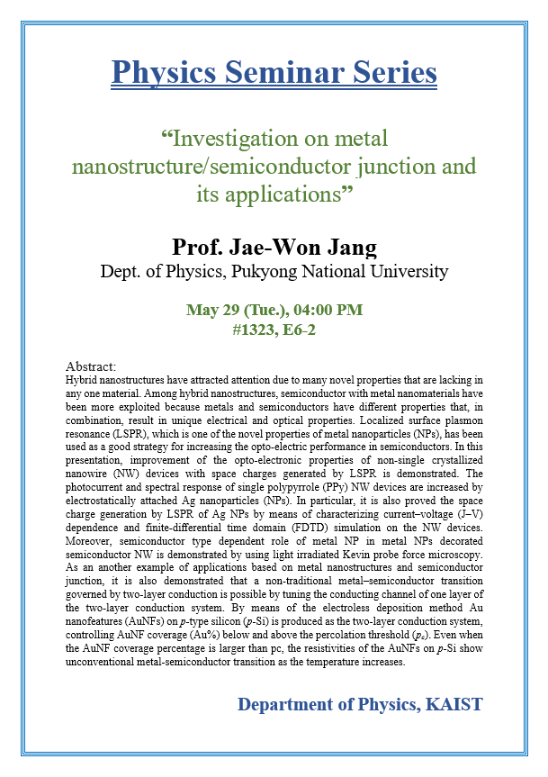
Physics Seminar Series
“Investigation on metal nanostructure/semiconductor junction and its applications”
Dept. of Physics, Pukyong National University
Abstract:
Hybrid nanostructures have attracted attention due to many novel properties that are lacking in any one material. Among hybrid nanostructures, semiconductor with metal nanomaterials have been more exploited because metals and semiconductors have different properties that, in combination, result in unique electrical and optical properties. Localized surface plasmon resonance (LSPR), which is one of the novel properties of metal nanoparticles (NPs), has been used as a good strategy for increasing the opto-electric performance in semiconductors. In this presentation, improvement of the opto-electronic properties of non-single crystallized nanowire (NW) devices with space charges generated by LSPR is demonstrated. The photocurrent and spectral response of single polypyrrole (PPy) NW devices are increased by electrostatically attached Ag nanoparticles (NPs). In particular, it is also proved the space charge generation by LSPR of Ag NPs by means of characterizing current–voltage (J–V) dependence and finite-differential time domain (FDTD) simulation on the NW devices. Moreover, semiconductor type dependent role of metal NP in metal NPs decorated semiconductor NW is demonstrated by using light irradiated Kevin probe force microscopy. As an another example of applications based on metal nanostructures and semiconductor junction, it is also demonstrated that a non-traditional metal–semiconductor transition governed by two-layer conduction is possible by tuning the conducting channel of one layer of the two-layer conduction system. By means of the electroless deposition method Au nanofeatures (AuNFs) on p-type silicon (p-Si) is produced as the two-layer conduction system, controlling AuNF coverage (Au%) below and above the percolation threshold (pc). Even when the AuNF coverage percentage is larger than pc, the resistivities of the AuNFs on p-Si show unconventional metal-semiconductor transition as the temperature increases.
Department of Physics, KAIST


